RESEARCH AREAS
Our current research interests include nano-photonics including the design and analysis of nano-photonic materials for the realization of wavelength and sub-wavelength scale optical elements,
- Inverse design and deep learning in nanophotonics
- Photonic neuromorphic computing
- Silicon Photonics
- Optical phased array, LiDAR
- Metasurfaces
- Photovoltaics
Below you can find more information about some of the listed research topics.
Development of neuromorphic photonics processor
We targeted to develop a silicon-based neuromorphic photonics integrated circuit, tailored for classification tasks.
This involved assembling a circuit with a 4-channel network input, a linear transformation for weight multiplication, and nonlinear activation.
We meticulously designed and fabricated test patterns for each part, integrating them into a photonic AI accelerator chip on a 220 nm SOI CMOS compatible platform.

Intelligent (Artificial Intelligence assisted) and Inverse design of nanophotonic and Silicon-Photonic circuits
The interaction of light with nanostructures that have variations in the refractive index on the order wavelength or sub-wavelength generates so many rich physical concepts that cannot be easily observed in conventional medium. As a result, researchers have shown an interest in the field of nanophotonics. For example, super-prisms, self-collimation, negative refraction, super-luminal light, slow light, cavities with high quality factors, lasers with low threshold currents, surface modes, super-continuum generation, the epsilon-near-zero medium and the Dirac cone are interesting research topics that can only be observed within carefully designed photonic media and structures. At this stage, it becomes crucial to have powerful numerical techniques that utilize optimization algorithms. We can divide design approaches into two parts: conventional and non-intuitive methods. The standard institutional approaches all depend on trial and error. However, non-intuitive approaches utilizing optimization algorithms have recently become popular. It is important to point out that non-intuitive methods possess advantages over the conventional methods. Advanced smart computational methods hold great potential to revolutionize development in many applications. They will make it feasible to use AI based algorithms to examine complex models to exploit the enormous parameter space in a highly efficient manner. Optimization methods search the full parameter space for each targeted task by minimizing the cost function, providing a more efficient framework for achieving complex functionalities and novel devices.
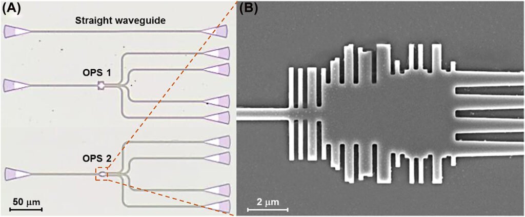
[Junhyeong Kim, Jae-Yong Kim, Jinhyeong Yoon, Hyeonho Yoon, Hyo-Hoon Park and Hamza Kurt, “Experimental demonstration of inverse-designed silicon integrated photonic power splitters,” Nanophotonics, 2022]
https://www.degruyter.com/document/doi/10.1515/nanoph-2022-0443/html
https://www.sciencedirect.com/science/article/pii/S0030401819307989
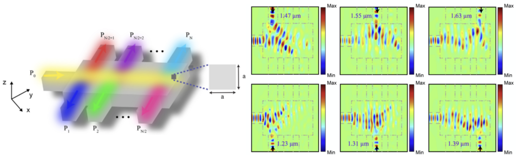
Integrated Optics in Silicon-on-Insulator Platform (Optical Phased Array LiDAR)
Light detection and ranging (LiDAR) is considered a promising solution for autonomous vehicles, drones, augmented or virtual reality displays, and camera sensors, among other applications requiring high-resolution range technology. LiDARs are active 2D and 3D sensors that illuminate the surroundings by emitting laser pulses. A precise range measurement and high spatial dimension information can be achieved by processing the received light pulse returning from the reflecting surface. Recently, research into solid-state LiDAR has emerged as a new technology that overcomes the shortcomings of conventional mechanical LiDAR. The silicon optical phased array (OPA) LiDAR is one of these solid-state LiDAR which have advantages in scanning speed, low power consumption, and compactness.
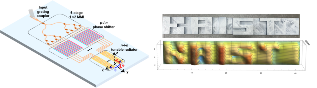
[Jinhyeong Yoon, Hyeonho Yoon, Jae-Yong Kim, Junhyeong kim, Hamza Kurt, and Hyo-Hoon Park, “Demonstration of high-accuracy 3D imaging using a Si optical phased array with a tunable radiator,” Optics Express 31 (6), 9935-9944, 2023]
Metasurfaces and flat optics
Recently, metasurfaces have been identified as promising optical elements in the modulation of the phase, amplitude and polarization of light within a subwavelength thickness. Compared to the bulky, conventional optical elements that use phase accumulation to manipulate light along curved optical paths, two-dimensional metasurfaces composed of engineered nanostructured antennas arrays allow the realization of the manipulation of light on a flat surface.Dielectric metasurface schemes pave the way to employing ultrathin metasurface elements to replace bulky, conventional optical elements with much lower power-loss and less fabrication complexity than plasmonic counterparts. When we compare light deflection and focusing scenarios by means of conventional optical elements, specifically refractive and diffractive optical elements, compared to a metasurface, a very thin layer of phase gradient enables superior light manipulation performances compared to conventional bulky ones.
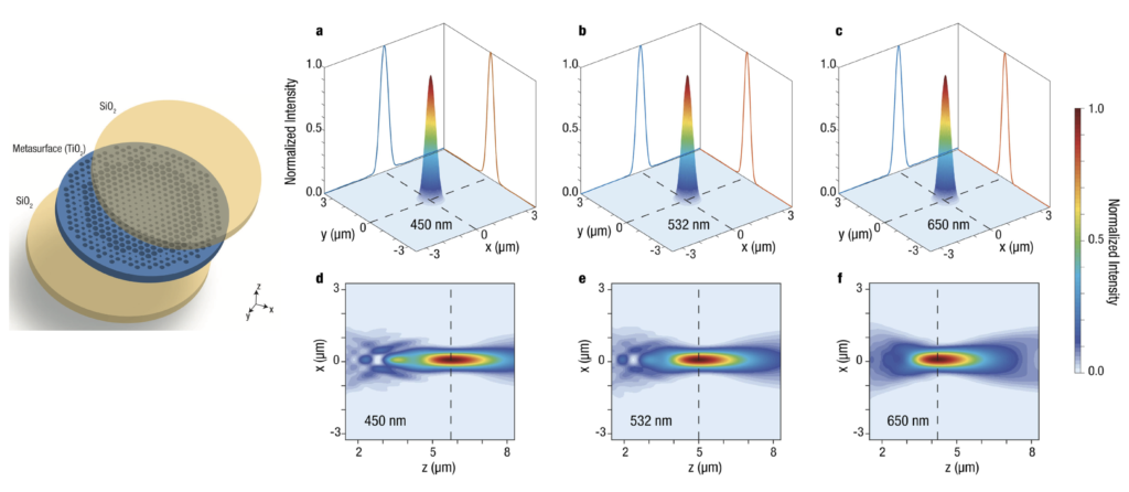
[N. Yilmaz, A. Ozer, A. Ozdemir, H. Kurt, “Nanohole-based phase gradient metasurfaces for light manipulation,” Journal of Physics D: Applied Physics 52 (20), 205102, 2019]
Parity-time optics, non-Hermitian photonics and topological photonics
Parity-time symmetry in optics is a condition whereby the real and imaginary parts of the refractive index are intentionally balanced across a photonic structure. The system experiences deviation from Hermiticity achieved by adding loss (attenuation) or gain (amplification) to an initially unitary (lossless) system. The balance between loss and gain leads to many interesting optical phenomena, including unidirectional invisibility, double refraction, power oscillations, single-mode lasing from multimode micro-resonators and non-reciprocal effects.
Topology in mathematics describes the properties of geometric space under deformations. The topological insulator is a special kind of insulator that has a typical insulating energy band structure, while a Dirac‐cone type of band structure appears in the band gap connecting the valance and conduction band. This peculiar characteristic of topological insulators results in surface (for 3D systems) or edge (for 2D systems) conduction, which is protected by topology and thus immune to disorder and defect. If achieved in an optical system, this ideal feature of conduction without dissipation and back‐scattering can be applied to the robust transport of light in photonic integration.
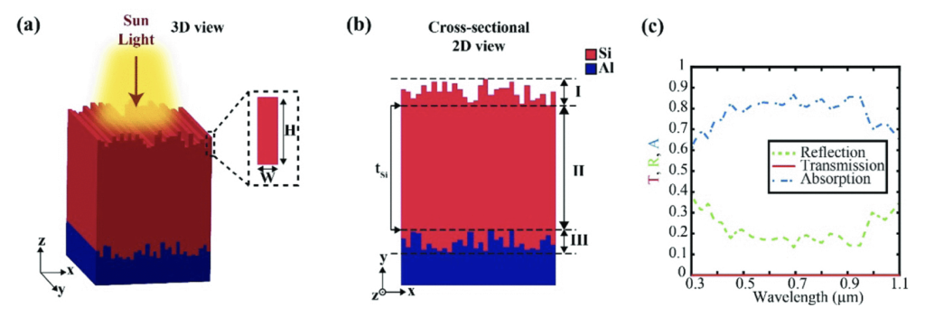
Photovoltaics: Light trapping and harvesting
One of the main limitations of thin-film silicon solar cells is their inability to capture a large portion of solar radiation due to the indirect band gap and low absorption coefficient of silicon. As a result, much research has been dedicated to the development of light-trapping methods for these devices. The aim of the current work is to incorporate smart nano-scale photon-management techniques that are neither insistent nor dependent on a single approach; instead, this research will thoroughly explore a plethora of novel methods to reach the highest efficiency in crystalline silicon solar cells. The tasks to achieve this can be divided into different objectives: suppression of reflection losses via high-index contrast surface corrugations and refractive index matching with 3D photonic structure, field-enhancement via slow-light concept to enhance absorption; light-focusing with an index-gradient concept; and optical-filtering based on the photonic band-gap property of a 3D photonic structure.
To harvest solar energy in an efficient and inexpensive way, the nano-scale management of photons is of paramount importance. In order to succeed in this goal, different strategies will be pursued in the current proposal. Once these design steps are performed by using numerical and analytical methods, fabrication and characterization of the designs will be carried out. The aim is to reach the theoretical efficiency limit of a single-junction solar cell. Due to the reduced thermal effects, the lifetime of the solar cell will be increased. The solar cell concentrator will allow a lesser amount of semiconductor material to be used. Consequently, the study will help in reducing the cost of photovoltaic technology.
[I. A. Atalay, H. A. Gunes, A. M. Alpkilic, and H. Kurt, “Multi-objective particle swarm optimization on ultra-thin silicon solar cells,” Journal of Optics 49 (4), 446-454, 2020]
In addition to these current research interest, we have performed studies on
- optical cloaking
- slow light
- graded-index optics
- low symmetric photonic crystals
- rainbow trapping of photons
- head-up display technology based on waveguide optics.